Thinner, smaller, and finer...
The photo-etching technology
which produces the world of the micron unit.
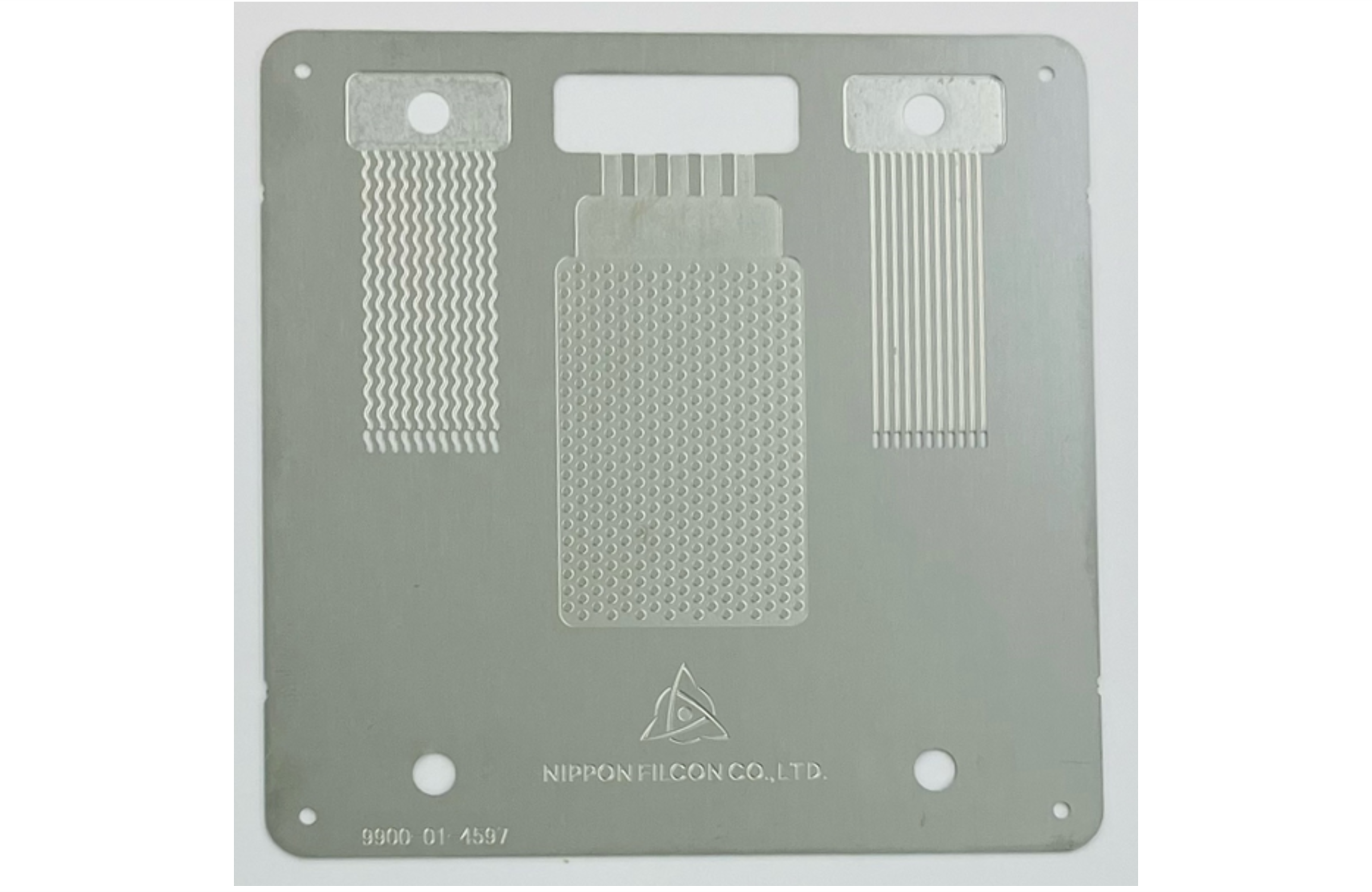
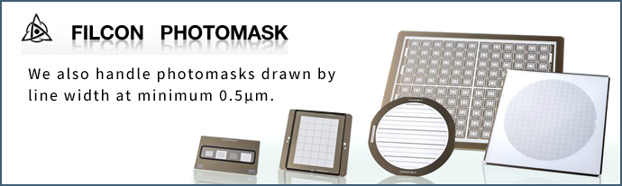
Examples of our products
At Nippon Filcon, we offer optimal processing methods,
such as metal etching, composite film etching, and roll-to-roll etching,
depending on your needs and intended use. Please feel free to contact us.

Our value
According to your demands, we have variable suggestions about from the selection and
development of materials to production and engineering based on much experience.
And, we'll take care of various products, from etching products to high-value-added products.
Metal etching
We can provide precision processing technology of metal etching at the micron unit.
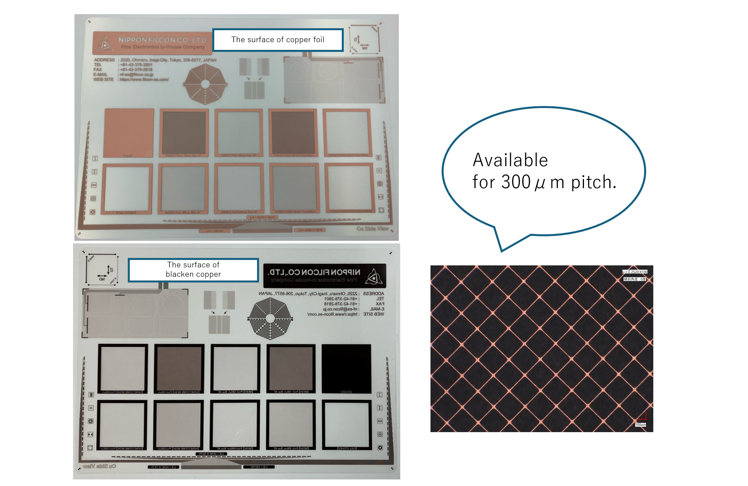
Composite film etching
We can suggest the etching services on various materials and uses based on processing technology of Cu/PET films.
We can deal with consistent processes from etching to secondary and third processing.
We aim to provide what our customer truly want by the combination
of not only precise etching process but also secondary and third processing.
Please feel free to contact us and we make the best suggestion.
(You can go to the web page of photomasks.)